The mask graphic data is skillfully crafted and submitted by the user, with subsequent processing handled by experienced engineers. Given the paramount importance of graphic data preparation in mask processing, utmost care is taken by users to meticulously examine all submitted layout files, thereby ensuring impeccable accuracy in the graphics.
Feature: Only a limited selection of products are displayed in the table. If you require other products, kindly consult our customer service team.
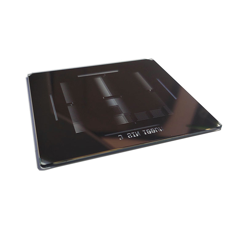
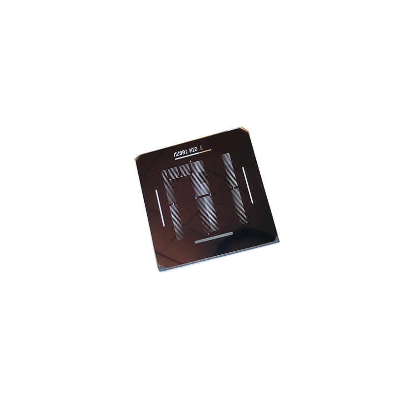
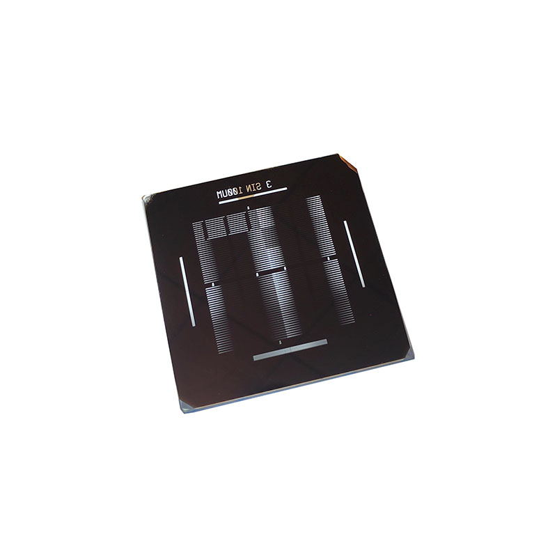
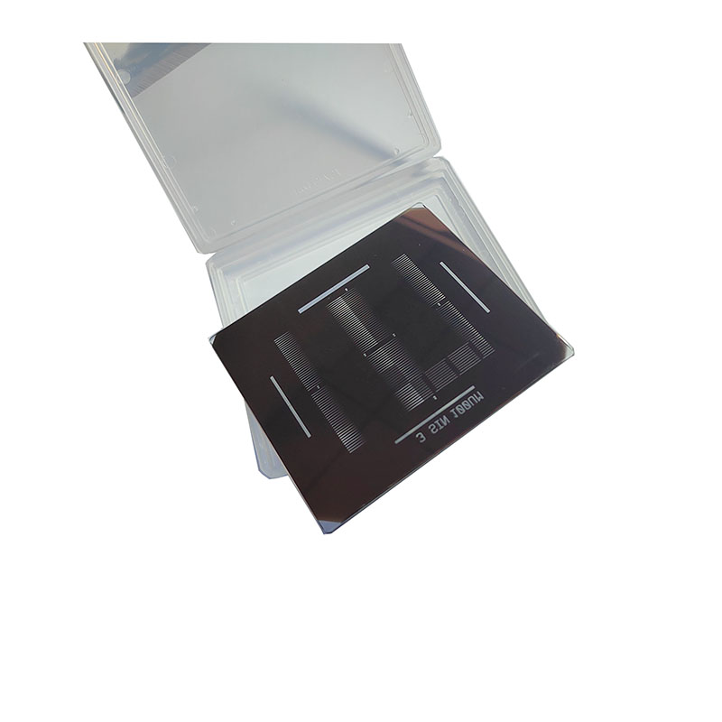
Physical Display of Quartz Glass Photomask Lithography Products
A lithography mask, alternatively known as a photomask or mask reticle, is a pattern master utilized in the lithography process, which is commonly used in micro-nano processing technology. The mask pattern structure is created on a transparent substrate using an opaque light-shielding film. Subsequently, the transfer of pattern information to the product substrate is achieved using the exposure process.
The mask is composed of a glass/quartz substrate, chromium layer, and photoresist layer and its pattern structure is obtained through a plate-making process. Direct-writing lithography equipment such as the laser direct-writing lithography machine is commonly used in processing the mask.
Masks find widespread use in fields involving lithography like IC (Integrated Circuit), FPD (Flat Panel Display), PCB (Printed Circuit Boards), and MEMS (Micro Electro Mechanical Systems).
Crafting Process:
1. Generate a mask reticle layout file (GDS format) conducive to the generation device.
2. Utilize a maskless lithography machine to read the layout file and perform non-contact exposure (exposure wavelength 405 nm) on the blank reticle with glue. This serves to illuminate the required pattern effect on the reticle such that the photoresist in the area undergoes a photochemical reaction (usually positive glue).
3. After developing and fixing, the photoresist in the exposed area dissolves and falls off, thereby exposing the underlying Chromium layer.
4. Utilize Chromium etching solution for wet etching and etch the exposed Chromium layer to form a light-transmitting area. The Chromium layer protected by the photoresist will not be etched, thereby forming an opaque area. This creates plane pattern structures with varying degrees of light transmittance.
5. If necessary, use dry or wet methods to remove the photoresist layer on the reticle and clean the reticle.
Exhibition Photos
Overall, we showcase a limited range of products in our table. However, our customer service team is readily available to provide professional assistance in meeting your specific needs. The physical display of our quartz glass photomask lithography products exemplifies our commitment to delivering high-quality and innovative solutions to the micro-nano processing technology industry. Our craftsmanship process emphasizes precision and attention to detail - no effort is spared in ensuring the quality of our products. Thank you for considering our products - we welcome the opportunity to work with you!
For inquiries about Machine Vision Calibration Board, Optical Glass Line Ruler, Photomask or price list, please leave your email to us and we will be in touch within 24 hours.
We use cookies to offer you a better browsing experience, analyze site traffic and personalize content. By using this site, you agree to our use of cookies.
Privacy Policy